

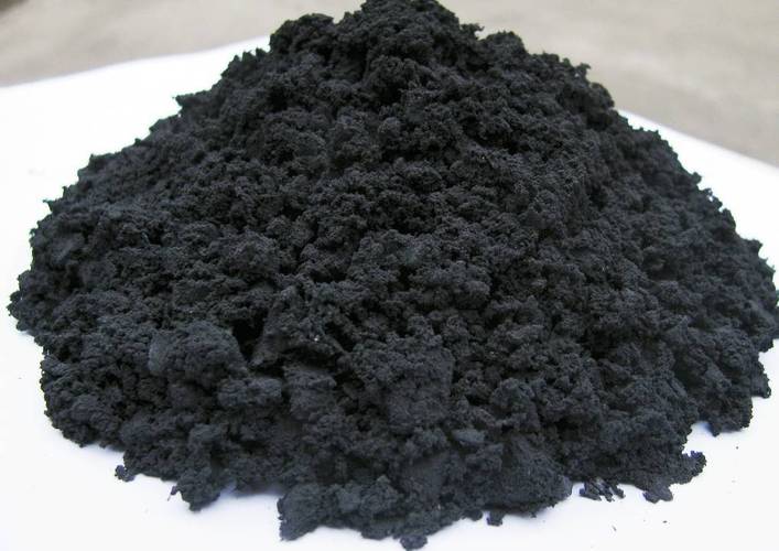
Graphene is one of the most promising materials in modern science and technology due to its exceptional properties such as high electrical conductivity, thermal conductivity, and mechanical strength. However, one of the challenges associated with working with graphene is achieving high-resolution imaging at small scales. Here’s how we can use optical microscopy to see atomically thin graphene layers without compromising on the quality of the image.
(how can we see atomically thin graphene layer using only optical microscope)
Optical microscopy is a technique that uses light to manipulate matter at the atomic or subatomic level. By shining a laser beam onto a sample, scientists can create an image of the material’s surface at different depths, revealing information about the structure and composition of the atoms and molecules within the sample. In the case of graphene, which has a very low density of atoms compared to other materials, optical microscopy offers a powerful tool for studying the material at atomic and molecular levels.
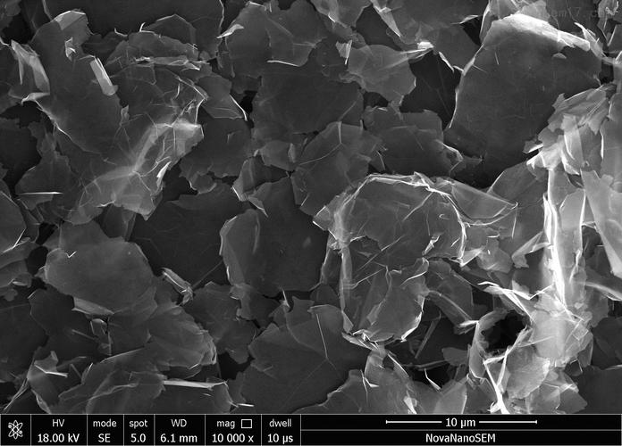
One of the key advantages of optical microscopy is that it allows scientists to obtain high-resolution images of graphene layers even at very small scales. For example, by using a microscope equipped with a scanning laser microscope (SLM), scientists can observe the individual atoms and molecules within a graphene sheet, down to sizes of a few nanometers. This is particularly important because graphene has a very low surface area, which means that the number of atoms and molecules per unit area is much higher than in other materials.
In addition to observing the surface of graphene layers, optical microscopy can also be used to study the structure and composition of individual atoms and molecules within the sample. By analyzing the interference patterns generated when light passes through a graphene sample, scientists can identify specific functional groups, defects, and other structural features of the material.
To achieve high-resolution imaging of atomically thin graphene layers using optical microscopy, several techniques must be employed. One approach is to use focused laser illumination, which focuses the laser beam onto a small spot on the graphene surface and projects it onto a detector array. By controlling the intensity and wavelength of the laser beam, scientists can optimize the focusing characteristics of the instrument to produce high-quality images.
Another important technique is to use spatially resolved confocal microscopy, which involves scanning the graphene surface in multiple directions simultaneously to capture multiple views of the material at different scales. This allows scientists to create detailed images of the structure and composition of individual atoms and molecules within the sample, without the need for expensive or time-consuming sequence acquisitions.
Finally, optical microscopy can also be used to analyze the interplay between the structure and composition of graphene layers. By analyzing the absorption and scattering properties of the material, scientists can gain insights into its electronic and optical properties, such as its charge carrier concentration, mobility, and dielectric constant.
(how can we see atomically thin graphene layer using only optical microscope)
Overall, optical microscopy provides a powerful tool for studying the properties and behavior of atomically thin graphene layers. By combining advanced imaging techniques with sophisticated computational tools, scientists can achieve high-resolution images of the material that can reveal new insights into its fundamental properties and potential applications. Whether working on research topics ranging from material design to electronics, or simply looking for ways to improve our understanding of this fascinating material, optical microscopy is an essential tool for advancing scientific knowledge in the field of materials science.
Inquiry us
